文章內容
Random Access Memory (RAM)


❒ Definition of RAM
Random Access means that the required time for data reading or writing of memory is not related to the position where the data is located. During usage, RAM can read data and can also write data. The most popular RAM now is SRAM and SDRAM. When the power is turned off, data will be immediately disappeared so RAM belongs to Volatile memory.
❒ Static RAM (SRAM)
SRAM uses six transistors (MOS) for storing one bit of data and does not need periodically supplying power during usage to maintain the content of memory, so it is called “static.” The structure of SRAM is complicated (requiring six transistors for storing one bit of data), so SRAM has faster access speed because of no capacitors and higher cost, and thus is generally produced as the memory requiring lower capacity but faster speed. For example, the cache memory of 256 KB, 512 KB, or 1MB built in a CPU usually employs SRAM.
❒ Dynamic RAM (DRAM)
DRAM uses one transistor (MOS) plus one capacitor for storing one bit of data and needs periodically supplying power during usage to maintain the content of memory, so it is called “dynamic.” The structure of DRAM is simpler (one transistor plus one capacitor.) Because the charging and discharging of capacitor requires longer time, the access speed is slower but the cost is lower. Thus, DRAM is generally produced as the memory requiring higher capacity but lower speed. Because the speed of CPU is faster and faster, the speed of conventional DRAM cannot meet the requirement, and thus DRAM has been currently replaced by SDRAM or DDR-SDRAM.
❒ Synchronous DRAM (SDRAM)
The clock should be the same while accessing data from CPU and SDRAM on motherboard, which is called “synchronous.” Because CPU does not have to “wait” during data access, it has higher efficiency. SDRAM has higher access speed than DRAM, so the computer motherboards in the early stage all employ SDRAM to replace conventional DRAM and currently only few industrial computers still employ DRAM.
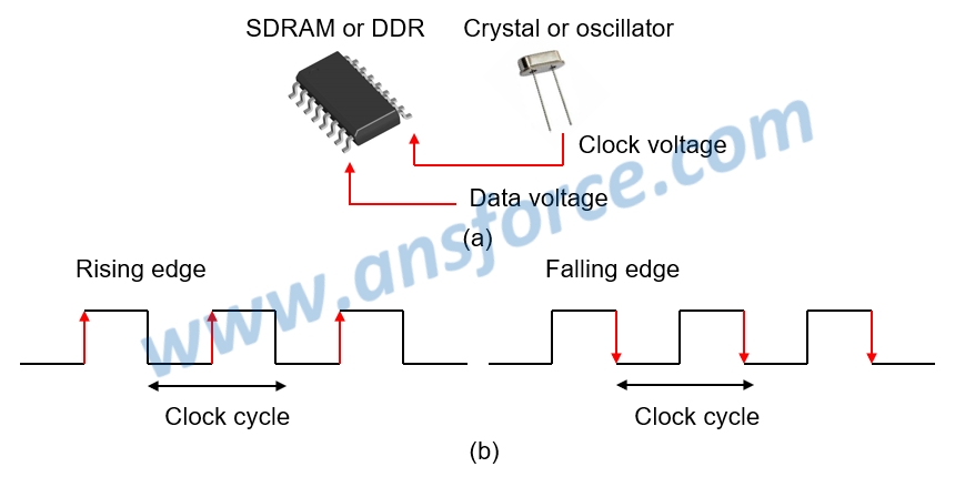
CPU and SDRAM are synchronized using the clock generated by crystal or oscillator. The crystal or oscillator is connected to a pin of SDRAM, as shown in Fig. 1(a), as the standard time for SDRM to read data. The clock generated by crystal oscillator is shown as Fig. 1(b) that the voltage is continuously changing between 1 V and 0 V.
➤ Rising edge: A rising edge is formed when the voltage is changed from 0 V to 1 V.
➤ Falling edge: A falling edge is formed when the voltage is changed from 1 V to 0 V.

Figure 1: Rising edge and Falling edge of Clock.
When SDRAM read a “rising edge,” it will transmit data to CPU; on the contrary, when SDRAM read a “falling edge,” it may possibly receive data from CPU. That is, CPU and SDRAM are synchronized for transmitting or receiving. Generally, transmitting or receiving is decided by another pin, which will not be discussed in detail herein.
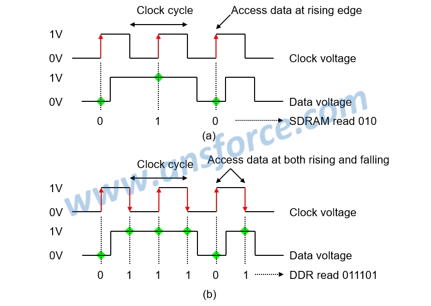
SDRAM accessed data when the clock is on the rising edge, which means to access data when the clock voltage is rising and not access data when the voltage is falling, so only one bit of data can be read in one clock, as shown in Fig. 2(a). Although the data voltage transmitted to SDRAM is kept changing, the digital data read by SDRAM can be confirmed as “010”(reading three bits) after synchronization with the rising edge of clock voltage.

Figure 2: Data access while SDRAM and DDR are matched.
There are different specifications for SDRAM while matching with the external frequency of CPU. For example, the operation frequency of SDRAM-200 is 200 MHz, and the data transmission rate is 1.6 GB/s, as shown in Fig. 1.
Table 1: Comparison of various SDRAMs.

❒ Double Data Rate SDRAM (DDR-SDRAM)
DDR-SDRAM can read two bits of data in one clock, so the operation speed is twice as SDRAM, called “Double Data Rate (DDR).” DDR only needs to slightly change the circuit of SDRAM to get doubled data access speed without increasing too much cost, so it immediately replaced SDRAM as the main stream product once launching on the market.
DDR can access data during both rising edge and falling edge of clock, that is, capable of accessing data when the clock voltage is rising and also accessing data when the voltage is falling, so it may read two bits of data in one clock, as shown in Fig. 2(b). Although the data voltage transmitted to DDR is kept changing, the digital data read by DDR can be confirmed as “011101”(reading six bits) after synchronization with the rising edge and falling edge of clock voltage. Obviously, the access speed of the same time will be twice as SDRAM.
There are different specifications for DDR while matching with the external frequency of CPU. For example, the operation frequency of DDR-400 is 200 MHz, but the data transmission rate may reach 3.2 GB/s, just twice faster than SDRAM-200, as shown in Fig. 1. The operation frequency of DDR may reach as high as 350 MHz (DDR-700).
➤DDR2: Because the operation speed of CPU for personal computer is faster and faster, scientists have developed faster DDR2 and DDR3 to increase many new functions for improving access speed that will not be described in detail herein due to too complicated principles. Basically, the data access speed of DDR2 is four times as SDRAM. For example, the operation frequency of DDR2-800 is 200 MHz, but the data transmission rate may reach 6.4 GB/s, just four times faster than SDRAM-200, as shown in Fig. 1. The operation frequency of DDR2 may reach as high as 300 MHz (DDR2-1200).
➤DDR3: The data access speed of DDR3 is eight times as SDRAM. For example, the operation frequency of DDR3-1600 is 200 MHz, but the data transmission rate may reach 6.4 GB/s, just eight times faster than SDRAM-200, as shown in Fig. 1. The operation frequency of DDR3 may reach as high as 275 MHz (DDR3-2200).
➤DDR4: The data access speed of DDR4 is sixteen times as SDRAM. For example, the operation frequency of DDR4-3200 is 200 MHz, but the data transmission rate may reach 25.6 GB/s, just sixteen times faster than SDRAM-200, as shown in Fig. 1.
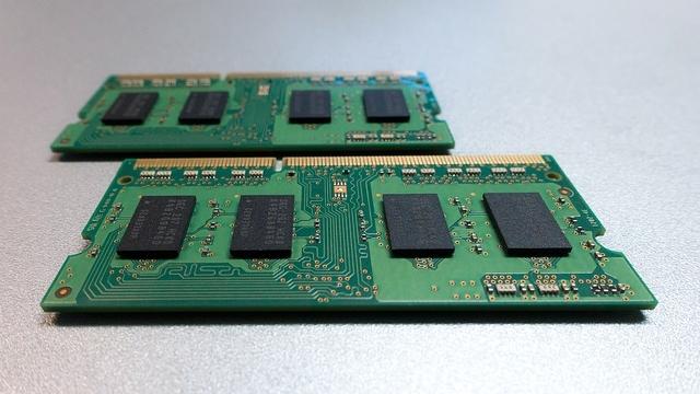
Moreover, Table 1 shows the development progress of DDR that the operation voltage is lower and lower, from 3.3V of SDRAM to 1.2V of DDR4; and, the date rate and data transmission rate is faster and faster, wherein “T/s” means Transfer per second, i.e. the number of transmissions per second. Because the data width is 64 bits, 64 bits (8 bytes) of data may be transmitted each time, so the data rate of DDR4 is 3.2 GT/s and the data transmission rate is 3.2 GT/s x 8 bytes = 25.6 GB/s. The appearance of DDR is shown in Fig.3. DDR, DDR2 and DDR3 have similar structures, and the only difference is the notch in the center of the pins to prevent the user from mistake of installation.

Figure 3: Appearance of DDR-SDRAM.
Source: Martini on https://commons.wikimedia.org/w/index.php?curid=8941276,
https://archive.org/details/ddr-ddr2-ddr3-ddr4.
❒ Mobile DDR (MDDR)
MDDR is also called Low Power DDR (LPDDR) and is one kind of DDR capable of reducing operation voltage for power saving. For example, the operation voltage of MDDR is reduced from 2.5V of DDR to 1.8V, and the operation voltage of MDDR2 is reduced from 1.8V of DDR to 1.2V. MDDR may be applied for handheld electronic products, such as tablet computer, smart phone, etc.
【Remark】The aforementioned contents have been appropriately simplified to be suitable for reading by the public, which might be slightly differentiated from the current industry situation. If you are the expert in this field and would like to give your opinions, please contact the writer. If you have any industrial and technical issues, please join the community for further discussion.
