文章內容
Magnetic RAM (MRAM)

❒ History of MRAM
Magnetic RAM (MRAM) was first announced by Honey International Inc. in 1997 having 1MB. Then, IBM, Infineon, Motorola, Sony, Toshiba, NEC, Samsung and other companies successively invested on the MRAM development. The structure of MRAM is totally different from the ordinary electric storage device that the data may still be kept after power-off. MRAM belongs to non-volatile memory and has all the advantages that the other storage devices have.
❒ Magnet and magnetic dipole
Magnet has both North pole (N-pole) and South pole (S-pole). Scientists imagine that there are infinite “small magnets” within the magnet and each small magnet has both N-pole and S-pole, as shown in Fig.1 (a). These small magnets are called “Magnet dipole.”
When the magnet dipoles inside a magnet are arranged in order, the N-poles of all magnet dipoles are facing upward resulting in that the N-pole of the entire magnet is facing upward. In order to simplify the complexity of diagram, we usually use one arrow to represent the magnetic pole and the direction of the arrow is defined as the N-pole of magnetic dipole, as shown in Fig. 1(b). The material having magnetic dipole is called “Magnetic materials.” The polarized direction and the direction of magnetic field have different definitions, as shown in Fig. 1(c):
➤ Polarized direction: defined as the direction from S-pole toward N-pole inside a magnet.
➤ Direction of magnetic field: defined as the direction from N-pole toward S-pole outside a magnet.
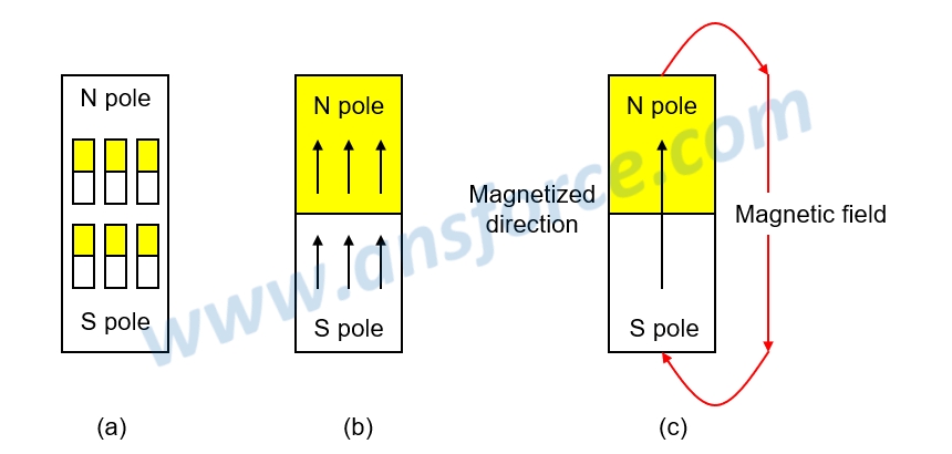
Figure 1: Magnet and Magnetic dipole.
❒ Magneto Resistance (MR)
When the material is affected by magnetic field, the phenomenon that the electric resistance is changed is called “Magneto resistance.” The common structure is shown in Fig.1. When the N-pole directions of two upper and lower layers of magnetic material are the same, the electric resistance is smaller (smaller voltage); and, when the N-pole directions of two upper and lower layers of magnetic material are opposite, the electric resistance is larger (larger voltage). Magnetic RAM utilizes electric current to generate magnetic field (Ampere’s right hand rule) to force the magnetic material generating different polarized directions to write data and use the magneto resistance to read data, so called “Magneto Resistive.”
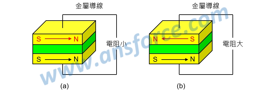
Figure 2: Principle of Magneto resistance.
❒ Structure of MRAM
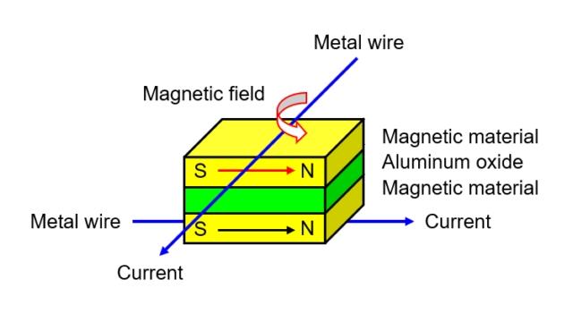
The structure of MRAM is shown in Fig. 3 that a layer of magnetic material (cobalt) is directly grown on a silicon wafer using sputtering; then, a layer of non-magnetic material (aluminum oxide, Al2O3) is grown again using sputtering; next, a layer of magnetic material (CoFe/NiFe) is grown again using sputtering; finally, a metal layer is grown using Chemical Vapor Deposition (CVD) method and using a photo mask, exposure, development and etching to etch the metal layer as metal wires. The metal wires must be distributed in each bit for accessing the data of each bit.
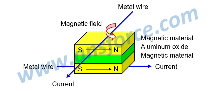
Figure 3: Structure of MRAM.
❒ Working principle of MRAM
The N-pole direction of lower layer magnetic material (Co) is fixed to the right. Based on Ampere’s right hand rule, the thumb indicates the current direction and other four fingers indicate the direction of magnetic field. The principle of data writing is shown in Fig. 4.
➤ Writing data 0: When the electric current flows on the metal wire above each bit from inward to outward, it may induce the upper layer magnetic material (CoFe/NiFe) to make N-pole toward to the right meaning writing data 0, as shown in Fig. 4(a).
➤ Writing data 1: When the electric current flows on the metal wire above each bit from outward to inward, it may induce the upper layer magnetic material (CoFe/NiFe) to make N-pole toward to the left meaning writing data 0, as shown in Fig. 4(b).
Please be noted that the writing method described as above only provides a rough concept. Because the method using magnetic field variation to change the polarized direction (N-pole direction) is not easily implemented on semiconductor circuit, currently in practice, the polarized direction is changed using voltage.
Data reading for MRAM utilizes the Magneto Resistance (MR) of magnetic material, which directly reads the data from the metal wire above and below each bit by measuring the voltages of upper layer magnetic material (CoFe/NiFe) and lower layer magnetic material (Co). The principle of data reading is shown in Fig. 4:
➤ Reading data 0: When the N-pole directions of upper and lower layers magnetic material are the same, the electric resistance is smaller (smaller voltage), as shown in Fig. 4(c).
➤ Reading data 1: When the N-pole directions of upper and lower layers magnetic material are opposite, the electric resistance is larger (larger voltage), as shown in Fig. 4(d).
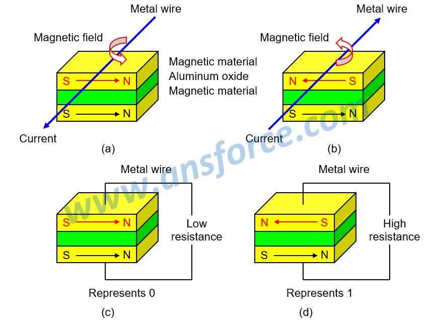
Figure 4: Working principle of MRAM.
❒ Advantages and Disadvantages of MRAM
➤ Advantages
1. MRAM belongs to non-volatile memory that the data may be still kept after power-off.
2. Not like Flash ROM requiring high voltage to force electrons injecting into floating gate, the power consumption of MRAM is lower.
3. Not like Hard Disk (HDD) requiring rotary motor and pick-up head, MRAM is very power saving, impact resistance, and without slipping.
➤ Disadvantages
1. MRAM must utilize various magnetic materials (FeCo/FeNi) that the manufacturing process is immature and the production yield is lower.
2. Many patent rights are held by foreign companies. The production cost is higher and the price is also higher due to license fee.
【Remark】The aforementioned contents have been appropriately simplified to be suitable for reading by the public, which might be slightly differentiated from the current industry situation. If you are the expert in this field and would like to give your opinions, please contact the writer. If you have any industrial and technical issues, please join the community for further discussion.
