文章內容
Flash ROM


❒ Definition of Flash ROM
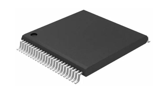
Flash ROM is currently the most popular portable electric storage device. Because Flash ROM is produced on a silicon chip using MOS processing, it has small volume and is very power saving and has been widely applied in all kinds of portable electronic products. Following the development of three-dimensional structure, a large amount of Flash ROMs has been applied on Solid State Disk (SSD).
❒ Structure of Flash ROM
The structure and working principle of Flash ROM are similar to EEP-ROM. As shown in Fig. 1, the thickness of the insulation layer of silicon oxide on the center P-type silicon wafer is thinner. The principle of data access is to use high voltage (usually above 10V) to make the electrons tunneling the silicon oxide from the N-type source on the left to be stored in the floating gate; then, using high voltage to attract the electrons in the floating gate to flow out of the N-type drain on the right. The difference is that Flash ROM utilizes a large block (usually kilo-bytes (KB)) as the basic unit for erasing data, so it is called “Flash.”.
➤ Source line: source of charges, because of using NMOS, the charges are electrons
➤ Bit line: for detecting if it is conducted; reading the bit to be 0 or 1.
➤ Word line: controlling the gate to control whether to create the electron channel below.
.jpg)
Figure 1: Structure of Flash ROM.
❒ Types of Flash ROM
➤ NOR flash: NOR flash has lower capacity, but faster access speed and higher price, so it is also called “Code storage flash.” As shown in Fig. 2(a), because the cell connection method is the same as NOR gate, so it is called NOR type and is generally used for storing software program requiring smaller amount of memory, for example, the boot-up program and operating system of mobile phone that can be executed in place (XIP: eXecute In Place).
Each cell of NOR flash is connected to bit line in a parallel connection that is convenient to randomly access each bit. NOR flash has dedicated bit lines for directly searching address at one time that can reduce the instruction execution time of the processor. For the same memory capacity, NOR flash has doubled size as NAND flash.
➤ NAND flash: NAND flash has higher capacity, but lower access speed and price, so it is also called “Data storage flash.” As shown in Fig. 2(b), because the cell connection method is the same as NAND gate, so it is called NAND type and is generally used for storing user’s database requiring large amount of data, for example, contact list of mobile phone, recording content of recorder pen, memory card for digital camera and digital video recorder, etc.
Each storage unit of NAND flash is connected to bit line in a serial connection divided into Bank, Plane, Block and Page. If each page is 512Byte, there is 512 x 8 bits, i.e. each page has 512 bit lines and each bit line has eight storage units.

Figure 2: Cell connection method of Flash ROM.
❒ Controller of NAND Flash
Although NAND flash cannot be randomly and rapidly accessed, this problem can be solved by modifying the control chip and greatly improving the access speed. Thus, currently the operating systems of all smart phones, for example, Androd, iOS, Windows phone, can be stored using NAND flash. What is the Flash ROM currently being used in the largest quantity worldwide? NOR flash or NAND flash? Because NOR flash is used for storing operating system for booting up, so the quantity is rather small; but, NAND flash is mainly used for storing data and the line width of manufacturing process is continuously reduced, so NAND flash above 32GB is now very popular. Thus, the one in the largest quantity is certainly NAND flash. Currently, NAND flash with large capacity may be even used to combine with control chip for replacing the conventional hard disk to be applied in tablet computer or notebook computer, which is called “Solid Stage Disk” (SSD).
❒ Charge Trap Flash (CTF)
The conventional flash memory utilizes polycrystalline silicon to produce the floating gate. However, the performance of polycrystalline silicon for charge storage is not so good, so the manufacturers utilized silicon nitride (SiN) film to replace polycrystalline silicon as floating gate having the same working principle as flash memory. In order to differentiate from the conventional flash memory, it was called a new name: Charge Trap Flash (CTF).
➤SONOS structure: Using silicon nitride (SiN) film to replace polycrystalline silicon as floating gate, being Polycrystalline silicon/SiN/SiN/SiN/Single crystal silicon from top to bottom, as shown in Fig. 3(a)
➤TANOS structure: A Charge Trap Flash is composed of Tantalum, Aluminum oxide, Nitride, Oxide and Silicon from top to bottom, as shown in Fig. 3(b).

Figure 3: Structure of Charge Trap Flash (CTF).
【Remark】The aforementioned contents have been appropriately simplified to be suitable for reading by the public, which might be slightly differentiated from the current industry situation. If you are the expert in this field and would like to give your opinions, please contact the writer. If you have any industrial and technical issues, please join the community for further discussion.
