文章內容
Image Sensor

❐ Structure of image sensor
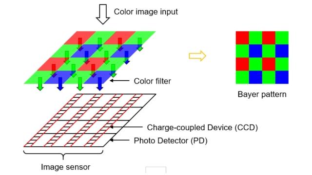
An image actually means a “frame” we saw, which is composed of many grids. The grids are called “pixels.” An image sensor is an array composed of many grids (pixels), and each pixel includes a Charge-coupled Device (CCD) and a photo detector (PD). Because a photo detector can only detect the brightness but cannot distinguish colors, a photo detector has to be mounted with a color filter to be able to obtain the color, as shown in Fig. 1(a). An image sensor has many types of RGB arrangements, in which the most common type is so-called Bayer pattern as shown in the figure. Have you noticed that the green pixels are two times of red and blue pixels in the Bayer pattern? Because human eyes are more sensitive to green color, it is reasonable to collect more information regarding green color.
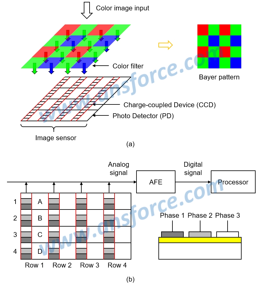
Figure 1: Structure and principle of CCD sensor.
❐ CCD image sensor
A Charge Coupled Device (CCD) is a device for pushing charges (electrons) moving forward, which utilizes three metal electrodes to push charges moving forward in sequence by different voltages. As shown in Fig. 1(b), the electrons in the photo detector of pixel A in the lower left corner will be pushed from 4 up to 3 by the adjacent CCD device; meanwhile, electrons of pixel B will be pushed from 3 to 2, electrons of pixel C will be pushed from 2 to 1, and electrons of pixel A will be pushed from 1 to the horizontal line; next, electrons of pixel A will be pushed from 3 to 2, electrons of pixel B will be pushed from 2 to 1, and electrons of pixel C will be pushed from 1 to the horizontal line, and so on. After the electrons of the first column were all pushed, the second column will be pushed, and then the third column will be pushed, and so on; wherein the electrons of each pixel in the image sensor must be sequentially pushed to the horizontal line. An Analog Front End (AFE) is used for converting the analog signal into the digital signal, i.e. an Analog to Digital Converter (ADC); then, the signal is inputted to a processor for digital signal processing.
As seen in the figure, the electrons of pixel A in the lower left corner need to be pushed four times to reach the horizontal line. For an image senor of a FHD frame having totally 1,920 x 1,080 = two millions of pixels, the first column has 1,080 pixels, so the electrons of pixel A in the lower left corner need to be pushed 1,080 times to reach the horizontal line. CCD is impossible to push all the charges 100%. Assuming one electron is lost while pushing 1,000 electrons by CCD and the incident light just enabled the pixel A in the lower left corner detecting 1,000 electrons, all electrons would be lost before reaching the horizontal line. Therefore, it is very difficult to produce CCD, so currently only Japanese manufacturers have the capabilities to design and produce CCDs and thus CCDs will be frequently out of stock while the price is high and money could not certainly buy.
The advantages of CCD image sensor are having better image quality and less noise; but the disadvantages are higher cost, higher power consumption, and that the AFE utilizes CMOS manufacturing process and cannot be integrated in the same chip as CCD due to different manufacturing process.
❐ CMOS image sensor
Complementary metal-oxide semiconductor (CMOS) is a switch device, wherein a gate is applied with positive voltage to form the electron channel below, so the electrons may be flowed in through the source and out through the drain. As shown in Fig. 2(b), the upper left corner of each pixel has a CMOS switch that the pixels may be sequentially turned on (conducted) one by one to enable the electrons in the photo detector flowing into the horizontal line in sequence, wherein the electrons of the first column will be running out, then the second column, the third column, and so on. The electrons of each pixel in the image sensor must be sequentially flowed to the horizontal line. The AFE is used for converting the analog signal into the digital signal, i.e. an ADC for the image; then, the signal is inputted to a processor for digital signal processing.
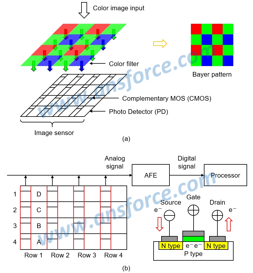
Figure 2: Structure and principle of CMOS sensor.
The advantages of CCD image sensor are low cost (approximately 1/3 of CCD), low power consumption (approximately 1/10 of CCD), and, most importantly, the AFE utilizes CMOS manufacturing process that is the same as the CMOS image sensor, so they can be integrated in the same chip to reduce the volume. This is very suitable to smart phone application, in which the device dimensions would be much concerned. The disadvantages of CCD image sensor are worse image quality and larger noise, especially the thermal noise generated by CMOS switch. The thermal noise will be generated above absolute zero degree (0K) and will be more severe for higher temperature. The frame of early stage CMOS image sensor would be seen few bright spots jumping around due to generation of thermal noise. Recently, because of progress of semiconductor processing, the noise problem of CMOS image sensor has been greatly improved.
❐ Image interpolation
Each pixel of an image display will present a color, which is composed by three primary colors of light, i.e. arrangement and combination of red, green and blue in different brightness. For example, FHD (Full High Definition) has 1,920 columns x 1,080 rows (about two millions of pixels), as shown in Fig. 3. Because each pixel of image display must be further divided into three RGB sub-pixels, a FHD display actually has totally six millions of secondary pixels, wherein the color of a certain pixel is arranged and combined by controlling the brightness of red (R), green (G), and blue (B).
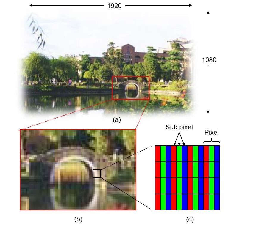
Figure 3: Each pixel of image display must be divided into three RGB sub-pixels.
Each pixel of image sensor can only detect the brightness, but cannot distinguish the color. In order to obtain the color, a color filter must be mounted on top of the image sensor, as shown in Fig. 1(a). An image sensor has many types of RGB arrangements, in which the most common type is so-called Bayer pattern as shown in the figure. Have you noticed that each pixel of image sensor has only one color but each pixel of image display could have three colors? What is the story?
In order to enable each pixel of image sensor having three colors, an image interpolation is now most commonly applied. That is, the average of colors of the pixels around a pixel is used to represent the values for other colors of this pixel. As shown in Fig. 4(a), the red brightness of a blue pixel may use the average of red pixels from four corners, and the green brightness may use the average of four surrounding green pixels; as shown in Fig. 4(b), the red brightness of a green pixel may use the average of the upper and lower red pixels, and the blue brightness may use the average of the left and right blue pixels. Then, every pixel on the image sensor may have brightness for all three RGB colors after calculation of image interpolation!
It should be noted that the three colors for each pixel of image sensor are obtained from calculation of image interpolation, which means that it is not the real color of this pixel, but only the average of other colors of the pixels around this pixel. Strictly speaking, for a digital camera having an image sensor with two millions of pixels and a HDTV (FHD=1,920 columns x 1,080 rows = two millions of pixels) having an image display with two millions of pixels, although they both have two millions of pixels, the real image quality of digital camera is only 1/3 of HDTV!
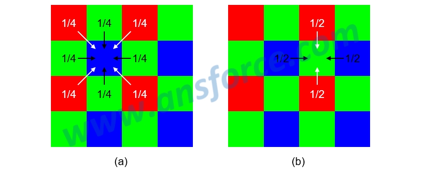
Figure 4: Calculation for image interpolation of image sensor.
【Remark】The aforementioned contents have been appropriately simplified to be suitable for reading by the public, which might be slightly differentiated from the current industry situation. If you are the expert in this field and would like to give your opinions, please contact the writer. If you have any industrial and technical issues, please join the community for further discussion.