文章內容
Photomask

❒ Making photomask
The photomask is a very important tool for producing Integrated Circuits (IC), which is made by shrinking the geometric pattern of millions of transistors (CMOS) at one time and writing onto a quartz sheet by electron beam. Because the diameter of electron beam is about 1μm, the pattern line width etched by electron beam on the quartz sheet is about 1μm.
The machine for etching the required pattern on a quartz sheet using electron beam for making a photomask is called “E beam writer.” This equipment is now manufactured by few international manufacturers, such as Applied Material, Lam Research. The making process of photomask is shown in Fig. 1, and described in details as follows:
➤ Metal sputter: Using sputter process to grow metal chromium (Cr) film on a quartz sheet, as shown in Fig. 1(a)
➤ Photoresist coating: Using photoresist coating machine to coat a photoresist layer on the surface, as shown in Fig. 1(b)
➤ Etching by electron beam: Directly applying electron beam to etch the photomask pattern on the photoresist, wherein the chemical bonds of photoresist within the area etched by electron beam will be broken, so the photoresist may be easily dissolved by chemicals, as shown in Fig. 1(c); because the diameter of electron beam is about 1μm, the pattern line width etched by electron beam is about 1μm.
➤ Chemical development: Using the first chemical (development solution) to dissolve the photoresist having its chemical bond broken, as shown in Fig. 1(d), wherein the development solution is usually organic chemical solvent
➤ Etching technology: Using the second chemical (etching solution) to dissolve the metal chromium (Cr) in the area without photoresist protection, as shown in Fig. 1(e); this process is called “Etching” ; wherein, the etching solution is usually corrosive strong acid, such as sulfuric acid, nitric acid, hydrochloric acid, hydrofluoric acid, etc.
➤ Photoresist removal: Using the third chemical (photoresist removal solution) to dissolve the remaining photoresist, as shown in Fig. 1(f); the photoresist removal solution is also organic chemical solvent but is different from the development solution. The time required for electron beam etching depends on the complexity of photomask pattern. The large-scale integrated circuit may have tens millions of transistors (CMOS), and the small-scale integrated circuit may have only hundreds of transistors (CMOS). The electron beam has to etch one by one, like an engraver working on a carved statue, so it takes very long time to complete, normally about tens of hours, and the price is very high.

Figure 1: Processes for making photomask.
❒ Functions of photomask
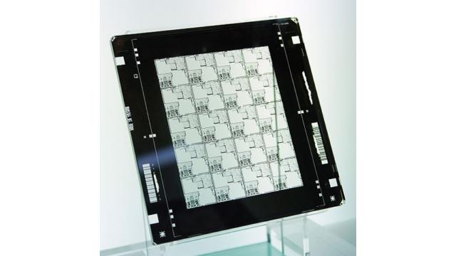
As seen in Fig. 2(a), the so-called photomask is actually a layer of metal chromium film attached on the surface of a quartz sheet, and this layer of thin film has an opening with the line width about 1μm. When the ultraviolet light irradiates onto the photomask, the area with chromium film will reflect the light like a mirror, but the area without chromium film (opening with line width about 1μm) will let the light penetrate the quartz sheet and to be projected below the photomask. If a convex lens for condensation is added below the photomask, an image the same as the photomask pattern but being smaller may be obtained. This is the method for shrinking the integrated circuit according to the design diagram. The actual appearance of photomask is shown in Fig. 2(b), wherein a photomask is overlapped with four identical photomask patterns for a chip and each photomask pattern has millions of CMOSs and fourteen different “function units.” Each function unit is responsible for one computing function. In Fig. 2(a), only one transistor (CMOS) in the photomask pattern is drawn for description.
.jpg)
Figure 2: Principle of photomask imaging.
【Remark】The aforementioned contents have been appropriately simplified to be suitable for reading by the public, which might be slightly differentiated from the current industry situation. If you are the expert in this field and would like to give your opinions, please contact the writer. If you have any industrial and technical issues, please join the community for further discussion.