文章內容
Thermal Diffusion


❒ Principle of thermal diffusion
The process utilizing high temperature to move the doping atoms in Si wafer and finally distribute them in suitable areas to form the desired structure is called “Thermal diffusion.” Thermal diffusion was often applied for process having larger line width and is described as follows. One type of atoms slowly moving within another type of atoms is called “diffusion.”
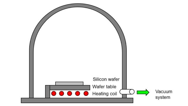
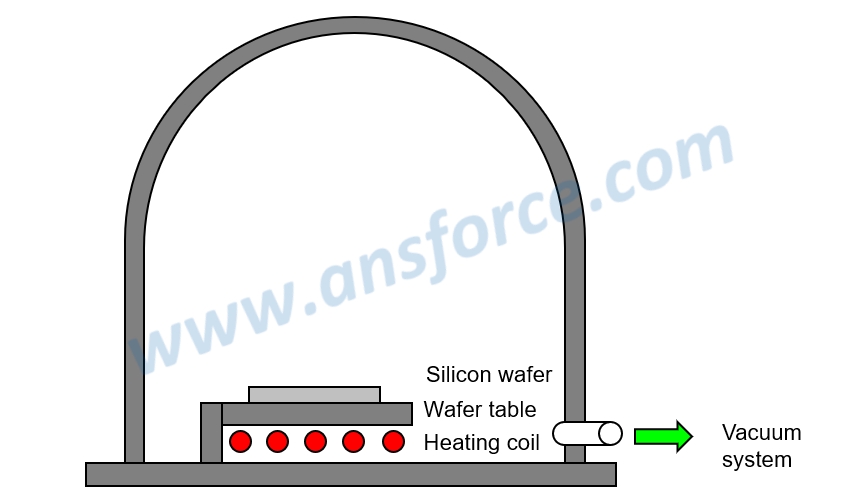
For example, a student sitting in the last row in classroom has worn perfume, and then the students sitting on the first row will smell the perfume later, because the perfume molecules are diffused in the air. Similarly, a drop of red ink is dripped in the water, and then the water in the whole tank will turn to red later, because the molecules of red ink are diffused in water. Diffusion is not only occurred in gas and liquid, but may also be occurred for solid atoms if the temperature is high enough. The diffusion for solid atoms will take longer time. Therefore, we can heat the solid to a very high temperature (hundreds of degree C) to diffuse solid atoms in Si wafer and thus achieve the purpose of doping. The machine used for thermal diffusion is called “high temperature furnace,” as shown in Fig. 1. The principle is quite simple that the doped atoms are evaporated on the surface of Si wafer and then heating in the high temperature furnace, so as to diffuse the doped atoms in Si wafer.

Figure 1: Structure and principle of high temperature furnace.
❒ Example of producing NMOS
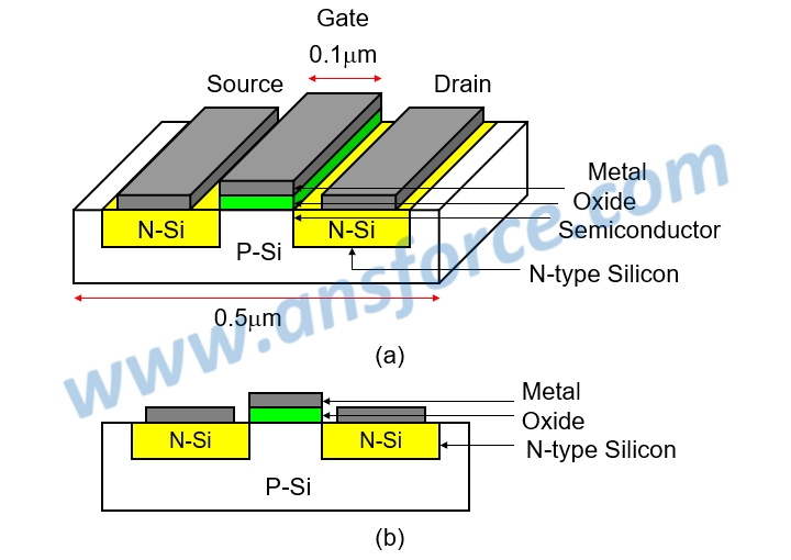
Here is an example for producing a NMOS on Si wafer using four processes, i.e. photolithography, doping, etching, and thin film growth. The structure of NMOS is shown in Fig. 2, which comprises three important structures and requires three photomasks to complete the process.
➤ First photomask: Preparing N-type regions respectively on left and right of P-type silicon substrate, like a trench structure, which must apply doping.
➤ Second photomask: Preparing a layer of silicon oxide on top of P-type silicon substrate at the center to form gates, which must apply etching.
➤ Third photomask: Evaporating a layer of metal copper electrode on top of silicon oxide at the center of P-type silicon substrate and on top of left and right N-type regions (trench), which must apply film growth.

Figure 2: Structure of NMOS.
It should be reminded that producing Integrated Circuit (IC) is not to produce CMOS one by one on Si wafer, but directly etching millions of CMOS on the photomask at one time; then, transferring the patterns with millions of CMOS using photolithography onto the dies of Si wafer at one time by the stepper. It takes shorter time, so the photomask may be used to rapidly transfer patterns onto Si wafer in a large amount.
❒ Application of thermal diffusion
The example utilizes the thermal diffusion to produce N-type regions respectively on left and right of P-type silicon substrate.
N-type region may be formed by doping a small amount of V-A group of atoms (N, P, As, Sb, Bi) in Si wafer. Making the example of doping P atoms, the process is shown in Fig. 3, and includes the following steps:
➤ Photoresist coating: Coating a photoresist layer on the surface using photoresist coater, as shown in Fig. 3(a).
➤ Photomask exposure: Next, using the first photomask for pattern transfer, wherein the patterns of the first photomask are penetrated by ultraviolet (UV) light through the left and right regions, as shown in Fig. 3(b). The chemical bonds of photoresists in the regions irradiated by UV light are broken, so the photoresist may be easily dissolved by chemicals.
➤ Chemical development: Using development solution to dissolve photoresist in an area having chemical bonds broken, as shown in Fig. 3(c).
➤ Film evaporation: Evaporating a layer of phosphorous film using film growth technology, as shown in Fig. 3(d).
➤ Photoresist removal: Dissolving the remained photoresist using photoresist removal solution and the phosphorous film thereon will also be removed by dissolution of photoresist, as shown in Fig. 3(e), only the region on top of the left and right regions is left with phosphorous film.
➤ Thermal diffusion: Using the high temperature furnace for heating; the phosphorous atoms are heated and slowly diffused into the silicon substrate to form two left and right N-type regions, as shown in Fig. 3(f).
.jpg)
Figure 3: Making N-type regions on left and right of P-type silicon substrate.
【Remark】The aforementioned contents have been appropriately simplified to be suitable for reading by the public, which might be slightly differentiated from the current industry situation. If you are the expert in this field and would like to give your opinions, please contact the writer. If you have any industrial and technical issues, please join the community for further discussion.
