文章內容
Ion Implantation


❒ Principle of Ion implantation
The process for directly injecting one type of atoms into Si wafer to distribute doping atoms in Si wafer is called “ion implantation,” just like directly firing a bullet into the wall. The doped atoms implanted into Si wafer may form two different types of semiconductors, i.e. N-type or N-type. This process is currently used for the advanced processing.
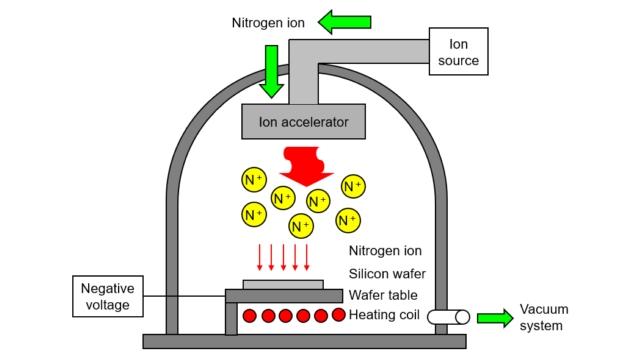
The process for directly injecting one type of atoms into Si wafer to distribute doping atoms in Si wafer is called “ion implantation,” just like directly firing a bullet into the wall. Because it is very difficult to directly accelerate the atoms to be injected into Si wafer, the gas atoms must first be applied with voltage to force electrons in the atoms jumping out to form gas ions (plasma) with positive charges. The process is called “ion implantation.” Furthermore, a negative voltage may be applied on Si wafer to attract the gas ions with positive charges to accelerate to be injected into Si wafer. The ion implantation method can achieve the same effect as the thermal diffusion; however, the gaseous ions must be formed using ion implantation, so the gaseous atoms must be used. The machine for ion implantation is called “ion implanter,” as shown in Fig. 1. The ion source may be applied with voltage to turn the gaseous atoms into gaseous ions; meanwhile, applying negative voltage on Si wafer to attract the gaseous ions with positive charges to accelerate to be downwardly injected into Si wafer.
.jpg)
Figure 1: Structure and principle of ion implanter.
❒ Example of producing NMOS
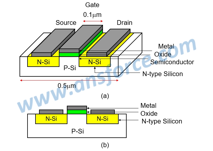
Here is an example for producing a NMOS on Si wafer using four processes, i.e. photolithography, doping, etching, and thin film growth. The structure of NMOS is shown in Fig. 2, which comprises three important structures and requires three masks to complete the process.
➤ First mask: Preparing N-type regions respectively on left and right of P-type silicon substrate, like a trench structure, which must apply doping.
➤ Second mask: Preparing a layer of silicon oxide on top of P-type silicon substrate at the center to form gates, which must apply etching.
➤ Third mask: Evaporating a layer of metal copper electrode on top of silicon oxide at the center of P-type silicon substrate and on top of left and right N-type regions (trench), which must apply film growth.

Figure 2: Structure of NMOS.
It should be reminded that producing Integrated Circuit (IC) is not to produce CMOS one by one on Si wafer, but directly etching millions of CMOS on the mask at one time; then, transferring the patterns with millions of CMOS using photolithography onto the dies of Si wafer at one time by the stepper. It takes shorter time, so the mask may be used to rapidly transfer patterns onto Si wafer in a large amount.
❒ Application of ion implantation
The example utilizes the ion implantation to produce N-type regions respectively on left and right of P-type silicon substrate.
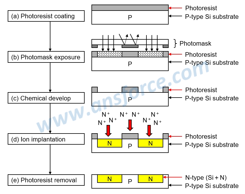
N-type region may be formed by doping a small amount of V-A group of atoms (N, P, As, Sb, Bi) in Si wafer. Making the example of doping nitrogen atoms, the process is shown in Fig. 3, and includes the following steps:
➤ Photoresist coating: Coating a photoresist layer on the surface using photoresist coater, as shown in Fig. 3(a)
➤ Mask exposure: Next, using the first mask for pattern transfer, wherein the patterns of the first mask are penetrated by ultraviolet (UV) light through the left and right regions, as shown in Fig. 3(b). The chemical bonds of photoresists in the regions irradiated by UV light are broken, so the photoresist may be easily dissolved by chemicals.
➤ Chemical development: Using development solution to dissolve photoresist in an area having chemical bonds broken, as shown in Fig. 3(c)
➤ Ion implantation: Evaporating a layer of phosphorous film using film growth technology, as shown in Fig. 3(d)Using ion implanter to generate nitrogen ions (plasma) with positive charges in the ion source; meanwhile, applying nitrogen ions with positive charges to accelerate to be injected into Si wafer, as shown in Fig. 3(d). In the areas without photoresist protection, the nitrogen ions will be directly injected into Si wafer to from two N-type regions on the left and right; and, the nitrogen ions in the areas with photoresist protection will be injected into the photoresist, but not into the Si wafer.
➤ Photoresist removal: Dissolving the remained photoresist using photoresist removal solution, as shown in Fig. 3(e).

Figure 3: Making N-type regions respectively on left and right of P-type silicon substrate.
❒ Comparison of thermal diffusion and ion implantation
➤ Thermal diffusion: Thermal diffusion is usually applied in the process with line width larger than 0.35μm. Because thermal diffusion belongs to “isotropic diffusion,” the doping atoms will not only diffuse downwardly in the diffusion, but also diffuse to the left and right, as shown in Fig. 4(a). The effect will not be so critical if the width of gate is larger than 0.35μm; but, if the width of gate is less than 0.35μm, the electron channel under the center gate of NMOS between two N-type regions will be too narrow, as shown in Fig. 4(b).
➤ Ion implantation: Ion implantation is usually applied in the process with line width less than 0.35μm. Because ion implantation belongs to “anisotropic diffusion,” the gaseous ions will only move downwardly during the process of injecting into Si wafer, but not move to the left and right, as shown in Fig. 4(c). No matter of the width of gate, the electron channel under the center gate of NMOS between two N-type regions is wide enough, as shown in Fig. 4(d).
.jpg)
Figure 4: Comparison of Thermal diffusion and Ion implantation.
【Remark】The aforementioned contents have been appropriately simplified to be suitable for reading by the public, which might be slightly differentiated from the current industry situation. If you are the expert in this field and would like to give your opinions, please contact the writer. If you have any industrial and technical issues, please join the community for further discussion.
