文章內容
Flip Chip Package (FCP)

❒ Process of Flip Chip Package
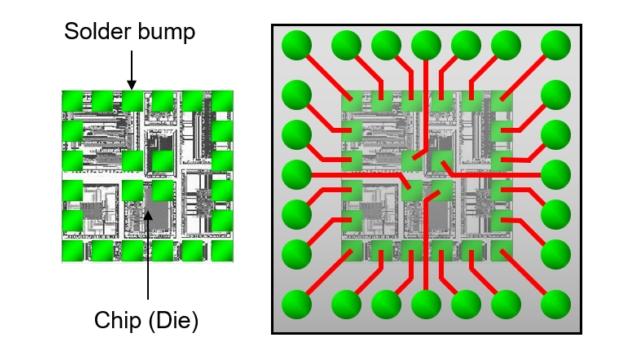
Flip Chip Package (FCP) normally utilizes “laminate substrate” and “solder bumps.” The solder bumps may be located anywhere on the chip, but not necessarily around the chip. The metal contacts on the laminate substrate may also be located anywhere on IC packaging case, but not necessarily around the case, as shown in Fig. 1. Therefore, there may be a lot of pins for flip-chip package. Furthermore, the flip-chip package needs no wire bonding, so the laminate substrate replaces the lead frame, and the solder bumps replace the gold wires.
The process of flip-chip package includes: making solder bumps on top of bond pad of chip; flipping the chip and heating to connect all solder bumps at one time with the metal contacts on the laminate substrate; and, finally filling adhesive (epoxy resin) to enclose the entire chip to protect the chip.
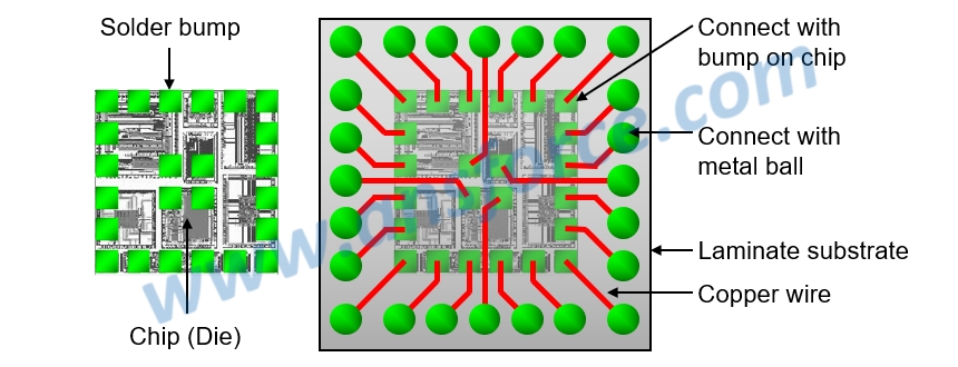
Figure 1: Flip-chip package.
The biggest advantage of flip-chip package is no need of wire bonding for IC interior packaging, because the operation of wire bonding must be processed one wire by one wire and it is very time consuming; but, the flip-chip package is to flip the chip and heating to connect all solder bumps at one time with the metal contacts on the laminate substrate, so as to complete the connection in a very short period of time.
❒ Applications of flip-chip package
Flip-chip package normally utilizes the “laminate substrate,” as shown in Fig. 2. The laminate substrate is used for connection with solder bumps on the chip. The IC package exterior using Pin Grid Array (PGA) or Ball Grid Array (BGA) is described as follows:
➤ Flip-chip package for interior and PGA for exterior: As shown in Fig. 2(a), this packaging method is now often applied for Intel CPU before.
➤ Flip-chip package for interior and BGA for exterior: As shown in Fig. 2(b), this packaging method is now often applied for Northbridge chip and Southbridge chip of personal computer.
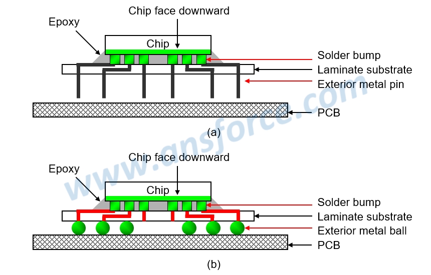
Figure 2: Application of flip-chip package.
❒ Advantage/Disadvantage of flip-chip package
➤ Advantage: Suitable for middle and small chips; no need of wire bonding so the speed is faster and the package volume is smaller.
➤ Disadvantage: The technical difficulty is higher, but now the technology is very mature.
【Remark】The aforementioned contents have been appropriately simplified to be suitable for reading by the public, which might be slightly differentiated from the current industry situation. If you are the expert in this field and would like to give your opinions, please contact the writer. If you have any industrial and technical issues, please join the community for further discussion.