文章內容
Chip Scale Package (CSP)

❒ Structure of Chip scale package
Chip Scale Package (CSP) may utilize “wire bonding” or “Flip Chip Package (FCP),” as shown in Fig. 1. The packaging process includes: directly making a very shallow indentation on a plastic card; using wire bonding or flip-chip package to connect the bond pads (metal bumps) on a chip with the metal contacts on a laminate substrate; and, filling adhesive (epoxy resin) into the indentation to protect the chip.
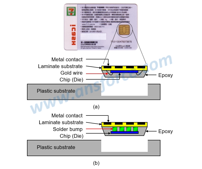
Figure 1: Appearance and structure of CSP.
Because currently the compact size has become a basic request for cell phones, more and more ICs for cell phones has applied the CSP. Besides, the popular chip card also belongs to CSP, such as IC telephone card, IC ATM card, IC credit card, Insurance IC card, Subscriber Identity Module (SIM) card of mobile phone, Memory card for digital camera, Smart card, non-contact sensing card for access control, etc. They all have a common feature that the volume after packaging is very small, so as to be placed into the thin plastic card.
❒ Advantage/Disadvantage of CSP
➤ Advantage: small volume after packaging, easy to carry and very low cost
➤ Disadvantage: very few pin number available, only suitable for small ICs, and poor chip protection effect
【Remark】The aforementioned contents have been appropriately simplified to be suitable for reading by the public, which might be slightly differentiated from the current industry situation. If you are the expert in this field and would like to give your opinions, please contact the writer. If you have any industrial and technical issues, please join the community for further discussion.