文章內容
Wafer Level Chip Size Package (WLCSP)


❒ Definition of WLCSP
The conventional packaging process is somewhat like a conventional machining process, i.e. using mechanical capillary for wire bonding, pressing and heating, but only being more precise. There is a new packaging technology that is conducted in a foundry to be directly applied on the wafer, so-called Wafer Level Chip Size Package (WLCSP).
The wafer level package means to first package the entire Si wafer and then perform the dicing operation. Because the volume after packaging will be increased less than 120% of the volume before packaging, it is also called Wafer Level Chip Size Package (WLCSP). WLCSP must satisfy the following two conditions:
➤ Dicing after packaging: Must first complete associated packaging and testing before die dicing.
➤ Similar to semiconductor processing: No need of conventional mechanical methods, like pressing, heating and bonding, but employing a process similar to semiconductor processing for packaging.
As described before, after a wafer has been produced in a foundry, there will be hundreds of exactly identical dies on the wafer. These dies must be diced along the cutting line by diamond cutter to form individual square chips; then, performing the packaging operation one by one. This is the defect of conventional packaging process, because the chips have to be packaged one by one and it is very time consuming. WLCSP is first to package the entire wafer and then perform the dicing operation. Obviously, WLCSP is more time saving, and the volume after packaging is almost the volume of chip. The package will be very small and is suitable for all kinds of compact handheld electronic products.
❒ Process of WLCSP
WLCSP is first to package the entire wafer and then perform the dicing operation. So, the packaging is conducted using a process similar to semiconductor processing. The process may be considered as the semiconductor processing introduced before. The process includes the following steps:
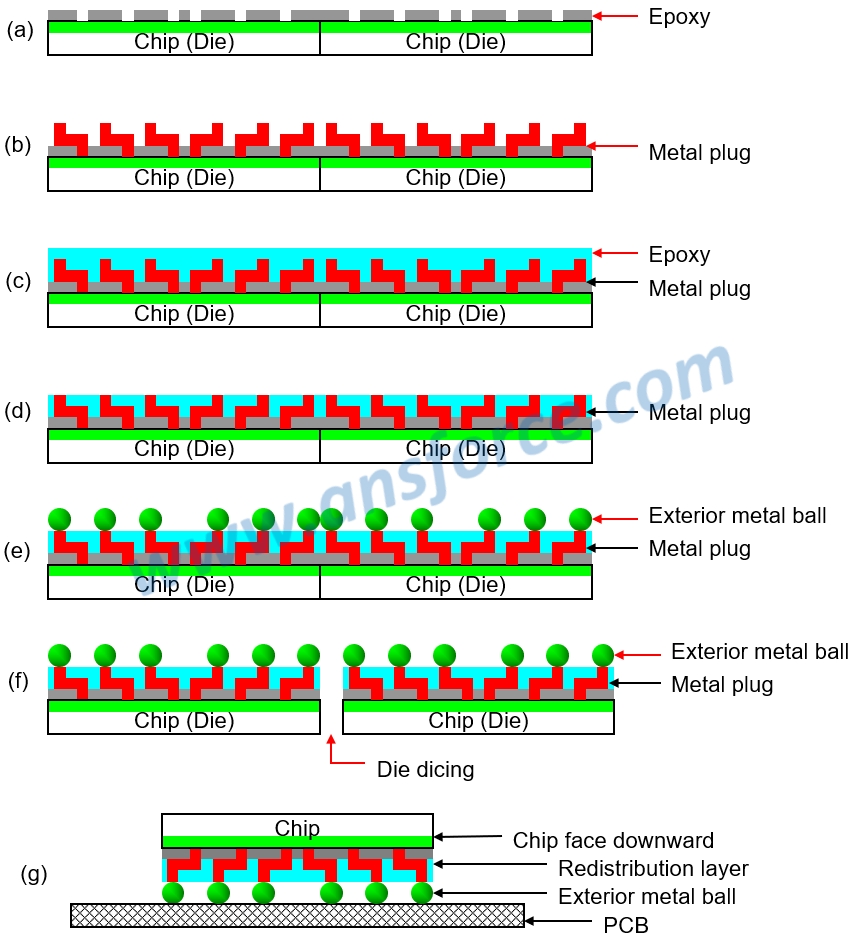
➤ Resin coating: After the processing for a wafer (before dicing by diamond cutter), using “spin coating” to coat a layer of epoxy resin on the entire surface of the wafer; then, removing the epoxy resin covered on the bond pads above the wafer by etching, as shown in Fig. 1(a).
➤ Metal evaporation: Using thin film growth technology to grow the metal film; then, using etching to remove the unwanted metal film forming metal plugs, as shown in Fig. 1(b).
➤ Resin coating: Using spin coating to further coat a layer of epoxy resin on the entire surface of the wafer for covering the metal plugs on the wafer and completely enclosing the metal plugs, as shown in Fig. 1(c).
➤ Surface polishing: Using Chemical Mechanical Polishing (CMP) to polish the epoxy resin and metal plugs on the entire surface of the wafer and expose the metal plugs in the bond pad area above the wafer; however, it is difficult to polish hard metal and soft resin at the same time, as shown in Fig. 1(d).
➤ Metal balls mounting: Using mechanical capillary to press and heat metal balls to be mounted at one time on the metal plugs exposed above the wafer; equivalent to external metal balls of conventional IC package, as shown in Fig. 1(e).
➤ Die dicing: Using diamond cutter to dice the wafer along the cutting lines to obtain the individual packaged ICs, as shown in Fig. 1(f).
The packaged IC may be connected to PCB, as shown in Fig. 1(g), as the ICs obtained by using the conventional packaging technologies. However, the volume after packaging is almost the same as the chip itself, so WLCSP is currently the packaging method having the smallest package volume.

Figure 1: Process flow of WLCSP.
This new packaging technology utilizes the processing technology in a foundry to be directly applied on a wafer, but it doesn’t mean that WLCSP has to be performed in a foundry, but might be performed in a packaging factory which may utilizes the processing in the foundry instead of the conventional mechanical processing, such as mask exposure, chemical development, etching, film growth, etc.
WLCSP cannot achieve good sealing effect. The back and the side of a chip are not under protection. Thus, we may apply epoxy resin or other plastic enclosure to achieve the sealing effect and protect the back of chip from scratching and also prevent the moisture and oxygen in the air from permeating onto the front surface of chip, so-called Encapsulated Wafer Level Chip Scale Package (eWLCSP).
❒ Advantage/Disadvantage of WLCSP
➤ Advantage: suitable for small ICs; lower cost due to no wire bonding; very small size after packaging suitable for IC products with strict volume requirement, such as cell phones and wearing type devices.
➤ Disadvantage: The technical difficulty is rather high and the process is different from the conventional packaging. Because the chip size is very small, there cannot have too many pins (solder balls) to be made within such a limited area, so WLCSP is not suitable for ICs with many pins.
【Remark】The aforementioned contents have been appropriately simplified to be suitable for reading by the public, which might be slightly differentiated from the current industry situation. If you are the expert in this field and would like to give your opinions, please contact the writer. If you have any industrial and technical issues, please join the community for further discussion.
