文章內容
FIWLP and FOWLP Packing


❐ Definition of FIWLP and FOWLP
Because the chip size is very small and there cannot have too many metal pins (solder balls) to be made within such a limited area, Wafer Level Package (WLP) is not suitable for ICs having too many pins. Thus, some companies have developed Fan-in Wafer Level Package (FIWLP) and Fan-out Wafer Level Package (FOWLP) to achiever lower cost and provide more pin number.
WLP has been developed over ten years, and there are many different types evolved therefrom, but all have the same basic principles. These types are only the transformation by improving the original processing.
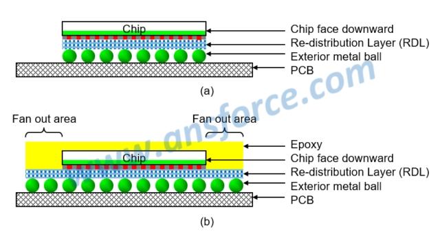
➤ Fan-in Wafer Level Package (FIWLP): Because the volume for WLP is very small and there cannot have too many metal pins (solder balls) made within such as limited area, normally the metal bumps on the top layer of the chip are made around the chip and the center area of the chip has no metal bump. In order to increase the number of metal pins (solder balls), the simplest method is to apply the “Re-distribution Layer (RDL) technology, which utilizes the metal re-distribution layer to inwardly spread the electric signals from the metal bumps around the chip to the center area of the chip, so as to increase the number of metal pins (solder balls), as shown in Fig. 1(a). Because the metal re-distribution layer is spread from outside to inside, it is called “Fan-in.”
➤ Fan-out Wafer Level Package (FOWLP): The “Fan-in” can utilize the metal re-distribution layer to inwardly spread the electric signals from the metal bumps around the chip to the center area of the chip. But, what if it is still not enough for electric signals? Then, the metal re-distribution layer may be further applied to outwardly spread the electric signals from the metal bumps around the chip to the area outside the chip. As shown in Fig. 1(b), because the metal re-distribution layer is spread from inside to outside, it is called “Fan-out.”
It should be noted that the original definition of WLP is that the associated packaging and testing must be finished before die dicing. However, for Fan-out, the dies must be diced first and then making the Re-distribution Layer (RDL). It seems to be not compliant with the definition of WLP, but it still employs the process similar to semiconductor processing, so we still classify this packaging method as WLP.
.jpg)
Figure 1: Illustration of Fan-in and Fan-out Wafer Level Package.
❐ Re-Distribution Layer (RDL)
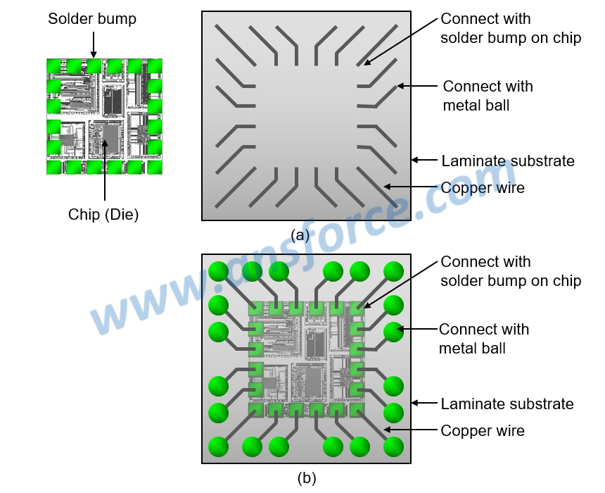
The structure of RDL is shown in Fig. 2. RDL is normally applied with flip-chip package and has the functions exactly the same as lead frame, i.e. spreading the aggregated electric signals, but different structure. The lead frame is to directly bend the metal pins as the shape of spider feet; but, the re-distribution layer utilizes the fabrication method of printed circuit board to bury metal circuits within a small piece of plastic board and the metal circuits have their one end aggregated and the other end spread out.
The IC packaging process is normally performed in a packaging factory. The conventional packaging process is somewhat like a conventional machining process, i.e. using mechanical capillary for wire bonding, pressing and heating, but only being more precise. This new type of packaging technology is directly performed on the wafer using the processing technology of a foundry, so it is called Wafer Level Package (WLP).

Figure 2: Structure of Re-distribution Layer (RDL).
❐ Process of Fan-out Wafer Level Package (FIWLP)
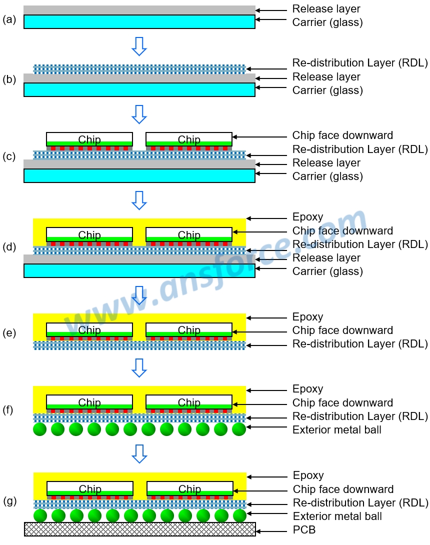
Fan-out WLP (FOWLP) must use a carrier to fix the chip. The most commonly used carrier is glass, because the glass has lower cost and is easily cut. The detailed process is shown in Fig. 3:
➤ Release layer: Using a glass substrate as carrier; coating a “release layer” thereon, as shown in Fig. 3(a), wherein the release layer is applied for easily separating the glass substrate from the re-distribution layer after finishing the processing
➤ Re-distribution layer: Attaching the re-distribution layer on the release layer, as shown in Fig. 3(b)
➤ Flip-chip package: Making metal bumps on the bond pads of the chip; flipping the chip and heating to connect all the metal bumps at one time with the metal contacts on the laminate substrate, so as to simultaneously perform the flip-chip packaging for many chips, as shown in Fig. 3(c)
➤ Molding: Filling adhesive (epoxy resin) to enclose the entire chip to protect the chip, as shown in Fig. 3(d)
➤ Carrier removal: Cutting the glass substrate into individual ICs; removing the release layer to separate the glass substrate from the re-distribution layer, wherein the glass substrate must be removed because it is only used for supporting during cutting, as shown in Fig. 3(e)
➤ Metal balls implantation: Connecting all the external metal balls at one tome with the metal contacts on the laminate substrate to complete the packaging process, as shown in Fig. 3(f); the package exterior is mostly applied with Ball Grid Array (BGA), so it is also called Embedded Wafer Level Ball Grid Array (eWLB).
Finally, the System Integrator (SI) will heat the packaged ICs and connect onto the PCB, as shown in Fig. 3(g). Because the re-distribution layer is spread in the Fan-out area from inside to outside, this method can increase the number of metal pins and the volume after packaging may be kept very small. Taiwan Semiconductor Manufacturing Corp. (TSMC) has successfully applied this simple technology to the domain of 3D chip packaging and successfully replaced Samsung for A10 processor orders by Apple in 2015 and has started the mass production in 2016 for iPhone 7.

Figure 3: Process of Fan-out Wafer Level Package (FOWLP).
【Remark】The aforementioned contents have been appropriately simplified to be suitable for reading by the public, which might be slightly differentiated from the current industry situation. If you are the expert in this field and would like to give your opinions, please contact the writer. If you have any industrial and technical issues, please join the community for further discussion.
