文章內容
Sputter

❒ Features of sputter
Sputter has no chemical reaction occurred in the process of film growth, so it belongs to Physical Vapor Deposition (PVD). Because sputter only needs High Vacuum (HV) and the evaporated film may be rapidly deposited on the substrate in a large amount, so the cost is lower and it’s suitable for mass production in factory. The biggest feature of sputter is that it can be applied for materials regardless of their melting points. Sputter is usually used for producing the metallic reflective film of optical discs, ex. CD or DVD, metal leads of integrated circuit, anti-ultraviolet film or multi-layer film on eyeglasses lens, thin film filter, etc.
❒ Processing flow of sputter
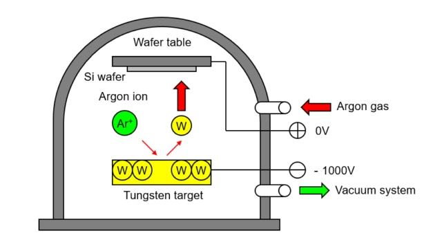
Making the example of growing tungsten (W) poly crystal film, as shown in Fig. 1, the processing steps are as follows:
1. Placing Si wafer under the positive electrode of sputter machine as substrate
2. Placing tungsten (W) solid blocks, called “target,” on the negative electrode (with negative charges)
3.Introducing argon gas (Ar) into the reactor and applying high electric field to form argon plasma, i.e. argon ions (with positive charges)
4. Argon ions (with positive charges) will be attracted by negative electrode (with negative charges) to impact the tungsten target so that the tungsten atoms may be knocked out.
5. Escaped tungsten atoms will move toward the Si wafer (substrate) and will be deposited on the substrate to form tungsten poly crystal film.

Figure 1: Illustration of sputter system.
The principle of sputtering is similar to billiards. The argon ions play like the “cue ball” and the tungsten atoms from tungsten target play like the “object balls.” The argon ions (cue ball) need only to knock out the tungsten atoms (object balls) without melting the tungsten target, so it is not related to the melting point of tungsten target. Sputter can be applied for materials regardless of their melting points. Some sputter machines may be designed with a “negative bias power supply” at the wafer table to attract the tungsten ions with positive charges injecting in high speed onto the Si wafer or substrate made of other materials, so as to greatly enhance the adhesion of thin film. Currently, most of the plastic eyeglasses lenses are grown with anti-ultraviolet film or multi-layer film by the sputter method.
【Remark】The aforementioned contents have been appropriately simplified to be suitable for reading by the public, which might be slightly differentiated from the current industry situation. If you are the expert in this field and would like to give your opinions, please contact the writer. If you have any industrial and technical issues, please join the community for further discussion.

